Vishay Isolated TrenchFET 2 Type P-Channel Power MOSFET, 1.1 A, 20 V Enhancement, 6-Pin SC-88 SI1967DH-T1-GE3
- RS Stock No.:
- 812-3108
- Mfr. Part No.:
- SI1967DH-T1-GE3
- Manufacturer:
- Vishay

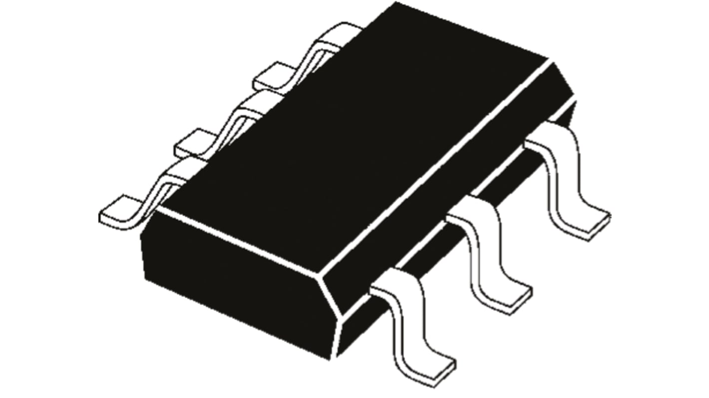
The image is for reference only, please refer to product details and specifications
Bulk discount available
View bulk pricing optionsSubtotal (1 tape of 50 units)*
HK$177.50
FREE delivery for orders over HK$250.00
In Stock
- 150 unit(s) ready to ship from another location
Need more? Click ‘Check delivery dates’ to find extra stock and lead times.
Units | Per unit | Per Tape* |
|---|---|---|
| 50 - 700 | HK$3.55 | HK$177.50 |
| 750 - 1450 | HK$3.49 | HK$174.50 |
| 1500 + | HK$3.424 | HK$171.20 |
*price indicative
- RS Stock No.:
- 812-3108
- Mfr. Part No.:
- SI1967DH-T1-GE3
- Manufacturer:
- Vishay
Specifications
Product overview and Technical data sheets
Legislation and Compliance
Product Details
Find similar products by selecting one or more attributes.
Select all | Attribute | Value |
|---|---|---|
| Brand | Vishay | |
| Channel Type | Type P | |
| Product Type | Power MOSFET | |
| Maximum Continuous Drain Current Id | 1.1A | |
| Maximum Drain Source Voltage Vds | 20V | |
| Package Type | SC-88 | |
| Series | TrenchFET | |
| Mount Type | Surface | |
| Pin Count | 6 | |
| Maximum Drain Source Resistance Rds | 790mΩ | |
| Channel Mode | Enhancement | |
| Minimum Operating Temperature | -55°C | |
| Typical Gate Charge Qg @ Vgs | 2.6nC | |
| Maximum Power Dissipation Pd | 1.25W | |
| Maximum Gate Source Voltage Vgs | 8V | |
| Transistor Configuration | Isolated | |
| Maximum Operating Temperature | 150°C | |
| Length | 2.2mm | |
| Height | 1mm | |
| Standards/Approvals | No | |
| Width | 1.35mm | |
| Number of Elements per Chip | 2 | |
| Automotive Standard | No | |
| Select all | ||
|---|---|---|
Brand Vishay | ||
Channel Type Type P | ||
Product Type Power MOSFET | ||
Maximum Continuous Drain Current Id 1.1A | ||
Maximum Drain Source Voltage Vds 20V | ||
Package Type SC-88 | ||
Series TrenchFET | ||
Mount Type Surface | ||
Pin Count 6 | ||
Maximum Drain Source Resistance Rds 790mΩ | ||
Channel Mode Enhancement | ||
Minimum Operating Temperature -55°C | ||
Typical Gate Charge Qg @ Vgs 2.6nC | ||
Maximum Power Dissipation Pd 1.25W | ||
Maximum Gate Source Voltage Vgs 8V | ||
Transistor Configuration Isolated | ||
Maximum Operating Temperature 150°C | ||
Length 2.2mm | ||
Height 1mm | ||
Standards/Approvals No | ||
Width 1.35mm | ||
Number of Elements per Chip 2 | ||
Automotive Standard No | ||
- COO (Country of Origin):
- CN
Vishay TrenchFET Series Power MOSFET, 20V Maximum Drain Source Voltage, 1.1A Maximum Continuous Drain Current - SI1967DH-T1-GE3
This power MOSFET is a P‑channel surface‑mount transistor designed for low‑voltage switching in Compact electronic systems. It operates as an enhancement‑mode device and is intended for board‑level power control where modest current handling and a small footprint are required.
Features and Benefits:
• 20V drain‑source rating enables low‑voltage system deployment • 1.1A continuous drain current supports light power switching • 790mΩ low Rds(on) reduces conduction losses during operation • 2.6nC typical gate charge permits Faster gate transitions • 1.25W power dissipation manages thermal load in small assemblies • Dual‑element isolated transistor allows paired switching arrangements
Applications
• Suitable for battery management and power rail switching in portable equipment • Ideal for load switching in industrial control modules • Used for reverse‑polarity protection in embedded systems • Can be used for signal level shifting in mixed‑voltage circuitry
What package should I plan for when designing the PCB?
The device is supplied in a 6‑pin SC‑88 SMD package that occupies a Compact footprint suitable for high‑density boards.
How does temperature affect operation limits?
The component is specified for operation between -55°C and 150°C, defining the allowable ambient and junction environments for reliable switching.
Can this component be used in automotive systems?
It is not classified to automotive standards, so suitability should be evaluated against vehicular qualification requirements before use.
What gate voltage range is permissible for control signals?
Gate drive must not exceed an 8V gate‑to‑source limit to avoid device overstress.
How many transistor elements are on the chip and what configuration are they?
The chip contains two isolated elements configured to enable paired or independent switching arrangements.
Related links
- Vishay Isolated TrenchFET 2 Type P-Channel Power MOSFET 20 V Enhancement, 6-Pin SC-88
- Vishay Isolated TrenchFET 2 Type N-Channel Power MOSFET 20 V Enhancement, 6-Pin SC-88
- Vishay Isolated TrenchFET 2 Type N-Channel Power MOSFET 20 V Enhancement, 6-Pin SC-88 SI1922EDH-T1-GE3
- Vishay Isolated TrenchFET 2 Type P 4.5 A 6-Pin SC-70
- Vishay Isolated TrenchFET 2 Type P 4.5 A 6-Pin SC-70 SIA517DJ-T1-GE3
- Vishay Isolated TrenchFET 2 Type P-Channel Power MOSFET 30 V Enhancement, 6-Pin TSOP
- Vishay Isolated TrenchFET 2 Type P-Channel Power MOSFET 30 V Enhancement, 6-Pin TSOP SI3993CDV-T1-GE3
- Vishay Isolated TrenchFET 2 Type P 135 mA 6-Pin SC-89-6 SI1025X-T1-GE3