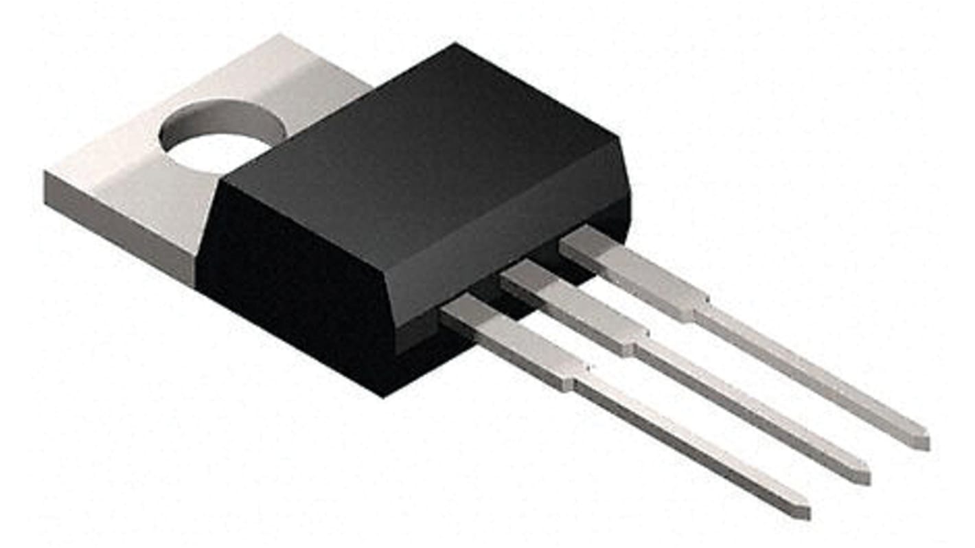
N-Channel MOSFET, 17 A, 650 V, 3-Pin TO-220 onsemi FCP190N65S3

- RS Stock No.:
- 172-4632
- Mfr. Part No.:
- FCP190N65S3
- Manufacturer:
- onsemi
20 In stock for delivery within 3 working days
Added
Price Each (In a Pack of 10)
HK$24.981
| Units | Per unit | Per Pack* |
| 10 - 190 | HK$24.981 | HK$249.81 |
| 200 - 390 | HK$24.356 | HK$243.56 |
| 400 + | HK$23.981 | HK$239.81 |
| *price indicative | ||
- RS Stock No.:
- 172-4632
- Mfr. Part No.:
- FCP190N65S3
- Manufacturer:
- onsemi
Product overview and Technical data sheets
Legislation and Compliance
- COO (Country of Origin):
- CN
Product Details
SuperFET® III MOSFET is ON Semiconductor’s brand-new high voltage super-junction (SJ) MOSFET family that is utilizing charge balance technology for outstanding low on-resistance and lower gate charge performance. This advanced technology is tailored to minimize conduction loss, provide superior switching performance, and withstand extreme dv/dt rate. Consequently, SuperFET III MOSFET is very suitable for various power system for miniaturization and higher efficiency.
700 V @ TJ = 150 oC
Higher system reliability at low temperature operation
Ultra Low Gate Charge (Typ. Qg = 30 nC)
Lower switching loss
Low Effective Output Capacitance (Typ. Coss(eff.) = 277 pF)
Lower switching loss
Optimized Capacitance
Lower peak Vds and lower Vgs oscillation
Internal Gate resistance: 7.0 ohm
Lower peak Vds and lower Vgs oscillation
Typ. RDS(on) = 170 mΩ
For products that are Customized and under Non-cancellable & Non-returnable, Sales & Conditions apply.
Specifications
Attribute | Value |
|---|---|
| Channel Type | N |
| Maximum Continuous Drain Current | 17 A |
| Maximum Drain Source Voltage | 650 V |
| Package Type | TO-220 |
| Mounting Type | Through Hole |
| Pin Count | 3 |
| Maximum Drain Source Resistance | 190 mΩ |
| Channel Mode | Enhancement |
| Maximum Gate Threshold Voltage | 4.5V |
| Minimum Gate Threshold Voltage | 2.5V |
| Maximum Power Dissipation | 144 W |
| Transistor Configuration | Single |
| Maximum Gate Source Voltage | ±30 V |
| Width | 4.7mm |
| Number of Elements per Chip | 1 |
| Length | 10.67mm |
| Typical Gate Charge @ Vgs | 33 nC @ 10 V |
| Maximum Operating Temperature | +150 °C |
| Forward Diode Voltage | 1.2V |
| Minimum Operating Temperature | -55 °C |
| Height | 16.3mm |