Altera FPGA 5CSEMA6F31C8N, Cyclone V SE 110000 Cells, 110000 Gates, 5761K, 41509 Blocks, 896-Pin FBGA
- RS Stock No.:
- 830-3574P
- Mfr. Part No.:
- 5CSEMA6F31C8N
- Manufacturer:
- Altera

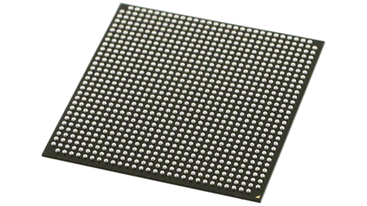
The image is for reference only, please refer to product details and specifications
Currently unavailable
We don't know if this item will be back in stock, RS intend to remove it from our range soon.
- RS Stock No.:
- 830-3574P
- Mfr. Part No.:
- 5CSEMA6F31C8N
- Manufacturer:
- Altera
Specifications
Product overview and Technical data sheets
Legislation and Compliance
Product Details
Find similar products by selecting one or more attributes.
Select all | Attribute | Value |
|---|---|---|
| Brand | Altera | |
| Family Name | Cyclone V SE | |
| Number of Logic Gates | 110000 | |
| Number of Logic Cells | 110000 | |
| Number of Logic Units | 41509 | |
| Dedicated DSP | Yes | |
| Number of Registers | 166036 | |
| Number of Multipliers | 224 (18 x 18) | |
| Mounting Type | Surface Mount | |
| Package Type | FBGA | |
| Pin Count | 896 | |
| Number of RAM Bits | 5761K | |
| Length | 31mm | |
| Maximum Operating Temperature | +85 °C | |
| Minimum Operating Temperature | 0 °C | |
| Width | 31mm | |
| Minimum Operating Supply Voltage | 1.8 V | |
| Maximum Operating Supply Voltage | 3.3 V | |
| Select all | ||
|---|---|---|
Brand Altera | ||
Family Name Cyclone V SE | ||
Number of Logic Gates 110000 | ||
Number of Logic Cells 110000 | ||
Number of Logic Units 41509 | ||
Dedicated DSP Yes | ||
Number of Registers 166036 | ||
Number of Multipliers 224 (18 x 18) | ||
Mounting Type Surface Mount | ||
Package Type FBGA | ||
Pin Count 896 | ||
Number of RAM Bits 5761K | ||
Length 31mm | ||
Maximum Operating Temperature +85 °C | ||
Minimum Operating Temperature 0 °C | ||
Width 31mm | ||
Minimum Operating Supply Voltage 1.8 V | ||
Maximum Operating Supply Voltage 3.3 V | ||
Cyclone FPGA, Altera
For these non-cancellable (NC), and non-returnable (NR) products, Terms and Conditions apply.
An FPGA is a semiconductor device consisting of a matrix of Configurable Logic Blocks (CLBs) connected through programmable interconnects. The user determines these interconnections by programming SRAM. A CLB can be simple (AND, OR gates, etc) or complex (a block of RAM). The FPGA allows changes to be made to a design even after the device is soldered into a PCB.